 |
| October 17, 2017 | Volume 13 Issue 39 |
Designfax weekly eMagazine

Archives
Partners
Manufacturing Center
Product Spotlight
Modern Applications News
Metalworking Ideas For
Today's Job Shops
Tooling and Production
Strategies for large
metalworking plants
Engineer's Toolbox:
The multi-switch detection interface: integrated features for smaller, more efficient designs
By John Griffith, Automotive Systems Engineer, Texas Instruments
Automotive body control modules (BCMs) are electronic control units that manage numerous vehicle comfort, convenience, and lighting functions, including door locks, windows, chimes, closure sensors, interior and exterior lighting, wipers, and turn signals. Specifically, BCMs monitor different driver switches and control power to corresponding loads in a car, as shown in Figure 1.
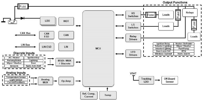
Figure 1: BCM block diagram.
A typical BCM consists of a microcontroller (MCU) that processes automotive 12-V battery level driver switch states. The signals connect to the MCU through interface circuits traditionally implemented using discrete passive components such as resistors, capacitors, and diodes. You must take care to protect the MCU from battery level voltages, electrostatic discharge (ESD), transients, and reverse-battery conditions. Additionally, you need to provide wetting currents for biasing the switch inputs and to keep the switch contact in good condition.
Figure 2 shows an example implementation of how to handle an external ground-connected switch input. Capacitor C2 shunts ESD and transient energy; diode D1 blocks high voltages; resistor R4 sets the wetting current at the switch; resistor R4 (in conjunction with R8) divides the battery level voltages down; and resistors R1 through R3, transistors Q1 and Q2, capacitor C1, and a general-purpose input/output (GPIO) pin enable and disable the wetting currents.
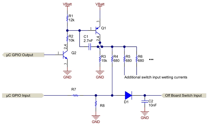
Figure 2: Discrete wetting current implementation.
There are three caveats to this discrete approach:
- The MCU, and therefore the MCU's supply voltage, have to remain active for the wetting currents to be active. This severely affects the minimum amount of current that the module consumes when in low power (key-off) mode.
- The solution requires a large number of passive components, such as transistors and resistors for creating the wetting currents, as well as diodes, resistors, and capacitors for each switch input. This makes the overall solution size large.
- The wetting current will vary with battery voltage; for example, if the battery voltage droops by 30%, the wetting current will also droop by 30%.
A multi-switch detection interface (MSDI) is a device that handles all of these issues, aggregating battery- and ground-connected switch status information and communicating back to a microprocessor via the serial peripheral interface (SPI).
Features for smaller, more space-efficient solutions
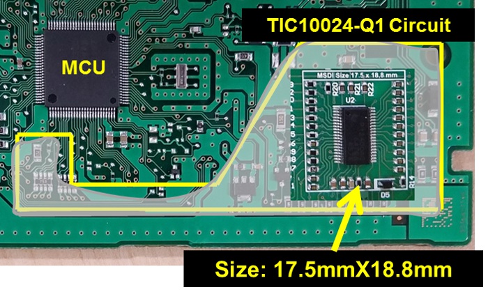
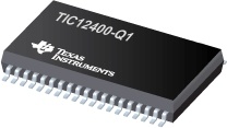
MSDI devices have integrated adjustable wetting currents capable of both sinking and sourcing currents for both battery- and ground-connected external switch inputs. Since these currents are internally monitored and controlled, they remain consistent over a wide range of battery input voltages. MSDI switch inputs are also designed to handle load dump and reverse-battery voltages, alleviating the need for discrete blocking diodes and wetting current components and thus saving additional board area and cost. A discrete 24-channel solution -- implemented as shown in Figure 2 -- would use 75 resistors, 25 capacitors, 24 diodes, and two external transistors. A comparable solution using the TI TIC12400-Q1 integrated MSDI solution would use 24 capacitors for IO pins, 5 capacitors for decoupling, a single resistor for the interrupt output, and a single MSDI device.
Figure 3 shows a 1-to-1 comparison of the solution size for discretely handling the wetting current, reverse blocking, and ESD on switch inputs and a snippet of the Automotive Multi-Switch Detection Interface reference design, which is an example implementation using the TIC12400-Q1 device with all of its required external circuitry. The total solution size on a two-layer board with the MSDI reference design is now 17.5 mm by 18.8 mm.
Features for more efficient low-power modes
As I mentioned before, to monitor an external switch in low-power mode, the microprocessor needs to remain powered on and active, meaning that the MCU's regulator also needs to remain active at all times. This results in higher system-wide quiescent current in low-power mode.
MSDI devices run directly off of car batteries and have an integrated low-power polling mode that makes it possible to monitor user-selected switch contacts. For example, the TIC12400-Q1 has a low-power polling mode and a high-voltage open-drain interrupt output pin that can enable a regulator upon a switch status change. This means that you can shut off all other circuitry in the module for an ultra-low-power sleep mode, helping meet tighter and tighter original equipment manufacturer (OEM) current requirements for sleep mode.
Figure 4 shows an oscilloscope screenshot where the TIC12400-Q1 is in low-power polling mode. Channel 1 shows the voltage at an open switch contact, and channel 2 shows the current consumption of the device.
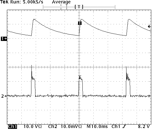
Figure 4: Low-power polling mode with switch monitoring
As you can see, the device is enabling the wetting current, monitoring the input voltage, and returning to low-power mode repeatedly while waiting for a switch contact to change state. This results in a much lower average current for the module, since all other circuitry in the module is disabled.
With the number of features in BCMs growing every year, the addition of an intelligent device like MSDI with integrated wetting currents, reverse blocking, and ESD protection helps enable smaller switch-contact monitoring solutions. In addition, as requirements for current consumption in low-power mode tighten, the integrated low-power polling mode in the TIC12400-Q1 enables system-wide power savings by as much as 98%.
------------------------------------------------------------
------------------------------------------------------------
SIDEBAR: Slash system power usage with TI's new fully integrated switch and sensor monitors
Texas Instruments (TI) recently introduced two multi-switch detection interface (MSDI) devices that consume up to 98% less system power than conventional discrete solutions. The TIC12400 and TIC12400-Q1 are the first switch and sensor monitors that directly interface with resistor-coded switches.
Manufacturers, especially automotive manufacturers, are challenged to integrate more functionality while saving power and space. The TIC12400 and TIC12400-Q1 can alleviate this challenge by natively monitoring the inputs and decoding the resistor path of as many as 54 switches in one device, offloading the signal decoding task from the processor. Additionally, by directly monitoring and providing built-in diagnostics for 24 channel inputs, the devices' polling sequence architecture reduces the system microcontroller active time, significantly cutting system power usage for applications including automotive body electronics and factory and building automation equipment.
Key features and benefits of the TIC12400-Q1:
- 98% lower system power: Designers can reduce system power consumption from milliamps to microamps in applications that need high efficiency. On-device monitoring allows the microcontroller to go into a low-power sleep mode and use less power when idle, which is essential for applications like automotive start/stop or when a car is parked for extended periods of time.
- Reduced complexity in a 60% smaller footprint: Eliminating up to 120 discrete components, the TIC12400-Q1 features an input-sharing and matrix mode that helps monitor 54 switches and sensors. The highly integrated device also includes adjustable wetting currents, timing controls, thresholds, and built-in redundant circuitry for protection, which increases system-level reliability by reducing potential points of failure.
- Robust, reliable system protection with simplified board layout: Integrated electrostatic discharge (ESD) protection and self-diagnostic features reduce external protection components. The new devices meet ISO 10605 ±8-kV ESD protection requirements, preventing potential fault events from damaging internal circuitry. The fully configurable devices independently monitor and protect 24 inputs, providing more headroom for the host microcontroller to perform other functions.
The TIC12400 evaluation module (TIC12400EVM-KIT) enables designers to quickly and easily evaluate the new device's capabilities. It is available from the TI store for $199.00.
Watch the TIC12400-Q1 in action here (scroll down once on new page).
This post (without sidebar) originally appeared on Texas Instruments' Behind the Wheel blog.
Published October 2017
Rate this article
View our terms of use and privacy policy